Geography of Silicon Chip
The
inputs processes and outputs of the creation of the silicon chip is:
Inputs
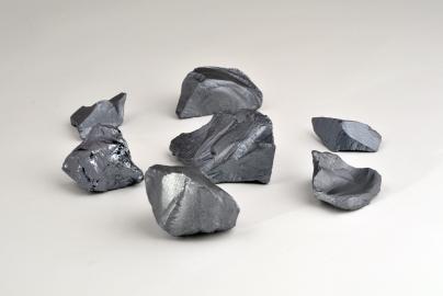
Silica
Sand
Copper
Hydrofluoric acid
Nitric acid
Processes
Heating in Furnaces
Fractional Distillation
Czochralski
Wire Saw
CVD
Chemical Mechanical Polishing
Outputs
Silicon Chip
Broken Silicon Chips
That is only to name a few inputs processes and outputs of
make the silicon chips.
FABs is the name given to the clean room facility that make the silicon due to tiny dirty particles destroying silicon chips. An example of these FABs is in Leixlip in County Kildare Ireland. Sit for Fabs are specially pick for flat stable ground and good transport to receive and transport goods and resource. These sit can cost Billions to build and run.
Silicon Chip are use all over the world in many devices from computer to even toys we use them every day but you now know how they are made.
I referenced
Intel Museum website
https://www-ssl.intel.com/content/www/us/en/history/museum-transistors-to-transformations-brochure.html
Tech Radar
http://www.techradar.com/news/computing-components/processors/how-sand-is-transformed-into-silicon-chips-599785
Intel Museum website
https://www-ssl.intel.com/content/www/us/en/history/museum-transistors-to-transformations-brochure.html
Tech Radar
http://www.techradar.com/news/computing-components/processors/how-sand-is-transformed-into-silicon-chips-599785
Earth Matters Folens by Eddie Guilmartin and Edwina Hynes